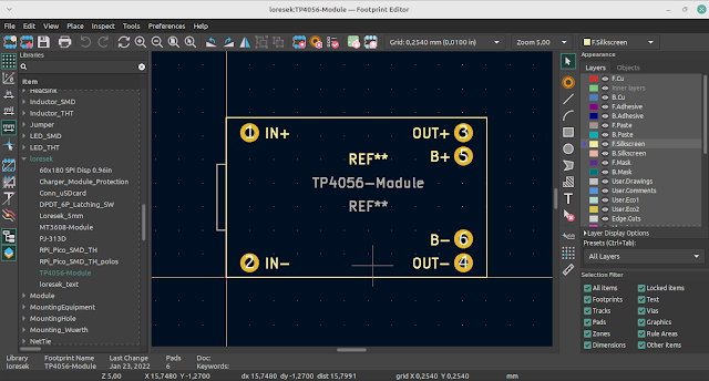
KiCAD Footprint: Conductive Pads

Kicad Conductive Pad footprints
These footprints are based loosly off the sizing that is used in the Gameboy Color and Pocket devices. In the schematic editor, assign these footprints using the common switch symbol.
If you need this footprint, follow the link below:
KiCAD Footprint: Conductive Pads