Creating a Coil Pattern in KiCad with Python - KiCAD Coil Creator
Create a coil pattern on a printed circuit board
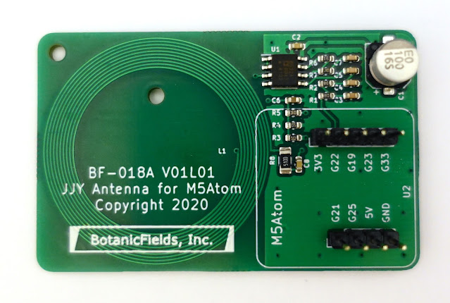
The following is a printed circuit board that emits pseudo radio waves (magnetic lines) resembling standard radio waves. The goal is to synchronize the time of a radio clock located in an area where radio waves do not reach. A current of 40/60kHz is passed through a spiral coil. I explored and attempted to create such a coil pattern in KiCad.
 |
| Coil Pattern created with KiCAD Coil Creator |
KiCad Coil Creator
Creating coil patterns in KiCad can be found in many examples by searching for "kicad coil" on the internet or GitHub. This time, I achieved good results using the KiCad Coil Creator.
Procedure
Get KiCad Coil Creator
Clone or download the GitHub repository below:
Edit Parameters in a Python Environment and Execute
I used Anaconda as the Python environment. Open the main.py of the KiCad Coil Creator via the Anaconda Prompt through the Idle Shell.
Edit the beginning part as follows:
For this coil, with an outer diameter of 35mm, there are 10 turns on both sides connected by inner vias. The coil part's width is as follows:
(Trace Width: 0.25mm + Width beetween trace: 0.25mm) X 10 Trun = 5mmWhen placing a via with a diameter of 0.8mm inside, the distance from the center to the via is as follows:
(Outer diameter: 35mm / 2) - 5mm - 0.8mm = 11.7mm
Running this code generates a 10-turn coil pattern at a distance of 11.7mm from the center, with vias as starting points, saved as a footprint file COIL_GENERATOR_1.kicad.mod.
Modify in KiCad Footprint Editor
Move the file COIL_GENERATOR_11.kicad.mod to a user folder, for example, under the following folder hierarchy:
C:\Users\username\Documents\KiCad\7.0\footprints\Modify COIL_GENERATOR_1.kicad.mod in KiCad's Footprint Editor.
This time, name the terminal as a round SMD Pad.
Connecting the coil part directly to the pad caused a problem with wiring on the printed circuit board. The attributes as a pad are only for the terminal part, and in the PCB Editor, the coil part is recognized as unconnectable. To solve this, add a Segment (straight line pattern) Primitive to connect the coil part to the SMD Pad.
Arrange in KiCad PCB Editor
Assign the modified Footprint to the PCB Editor, and perform placement and wiring by using KiCad's Schematic Editor's Footprint assignment tool.
When running DRC (Design Rules Checker) in the PCB Editor, errors may be detected inside the Footprint. In particular, the connection between the SMD Pad and the coil part can result in Clearance violation due to net mismatch. I tried various methods to resolve this error, but ultimately, it seems easiest for the designer to manually inspect and ignore all instances.
In Conclusion
KiCad has the unique feature of data being in a text format, allowing for modification and supplementation with external programs. Many people have created useful external programs and shared them. I am grateful to these individuals and would like to make effective use of their contributions.


