How to Simulate PCB Layouts for Crosstalk and Electromagnetic Interference
Transitioning from schematic to PCB layout introduces new challenges, mainly parasitic effects like trace impedance, capacitance, and inductance, which can cause electromagnetic interference (EMI) and crosstalk between traces. These issues can result in malfunctioning circuits, like random glitches or electrostatic discharge (ESD) that disrupt your board. While simulations like LTSpice can verify schematics, they don't account for these layout-induced issues. In this tutorial, I’ll guide you through verifying your PCB layout using free tools to check for crosstalk and magnetic emissions.
What You Need:
- KiCad 6.0 – Download KiCad to work with your PCB layout. It’s essential to use version 6.0 to avoid compatibility issues.
- FreeCAD – Version 0.19 is recommended for this tutorial.
- openEMS – This simulation tool will be used for electromagnetic field analysis. Follow the openEMS installation tutorial to get started.
- ParaView – Use this to visualize the simulation results.
Step-by-Step Guide:
Step 1: Prepare Your KiCad Layout
- Download the KiCad project (provided in the tutorial link) and extract it.
- Open the project in KiCad 6.0 and make sure the layout loads correctly before proceeding.
Step 2: Set Up FreeCAD for openEMS
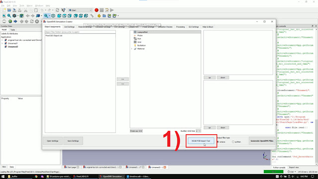
- Open FreeCAD and load the FreeCAD to openEMS macro. This macro helps integrate KiCad with openEMS for simulation. If you're unfamiliar with macros, be sure to watch the installation video beforehand.
 |
| Open Freecad and start the FreeCad to openEMS macro |
Step 3: Import KiCad Layout into FreeCAD
- In FreeCAD, click on the KiCad PCB Import Tool button.
- Select your KiCad project and check the "Fuse copper" box.
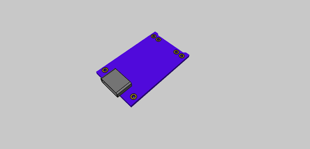
- Click Import KiCad PCB and wait for the process to complete. A message saying "all done" will appear once the import finishes.
Step 4: Simplify the 3D Model for Simulation
After importing, the model will have many parts. The goal is to simplify it:
- Expand coppers_drilled#F.Cu and move the child objects outside the parent.
- In the Parts Workbench, "fuse" the child objects and create a copy of the fused object.
- Copy the board_solid object (which represents the PCB) as well.
- Create a box to represent air around the PCB. The air box should be 1mm larger than the PCB in every direction.
- Copy the air box, shrink it, and place it between the top and bottom layers of the PCB. This will help measure the magnetic field inside the PCB.
Step 5: Set Up Simulation Parameters
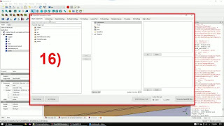
- Go to the Grid Settings tab and adjust the grid as shown in the tutorial.
- Under Material Settings, create materials for air and FR4 (with dielectric constants Epsilon = 1 for air, and Epsilon = 4.6 for FR4).
- In the Excitation Settings tab, create a step function for your signal input.
- Under Port Settings, create an active port with a signal strength of 1666V/m.
- Add a H-field probe to measure the magnetic field, which will give us insights into EMI.
- Set boundaries to PML (Perfectly Matched Layer), which simulates infinite space for accurate field propagation.
- Save your FreeCAD project and simulation settings.
Step 6: Run the openEMS Simulation
- After configuring everything, generate the openEMS files.
- Open the generated Python script (with a .py extension) and make necessary adjustments to the step function (if needed).
- Run the Python script to start the simulation. You’ll see a 3D preview of the simulation followed by the actual run in the command window.
Step 7: Visualize Results with ParaView
- After the simulation completes, open the output folder and launch ParaView.
- Load the simulation results (vtr files) into ParaView and adjust the color scale to visualize the magnetic field (H-field).
- You can optionally adjust the opacity of the copper trace layer to make the results clearer.
Step 8: Improve Your PCB Design for Better EMC
Once you have your simulation results, you can take steps to improve your layout and reduce EMI:
- Via Stitching: Make sure signals have return currents on all sides, especially where traces cross. Proper via placement can help reduce unwanted radiation.
- Switch to 4-Layer PCB: If your design suffers from crosstalk, switching to a 4-layer PCB can improve the ground plane's effectiveness and reduce EMI without too much effort.
- Reduce Trace Lengths: Shorter traces with fewer crossings reduce the chances of crosstalk and interference.
Video Version of Tutorial
Conclusion
By simulating your PCB layout for crosstalk and electromagnetic emissions, you can ensure your design works reliably even in complex environments. Using tools like KiCad, FreeCAD, openEMS, and ParaView, you can visualize and mitigate issues before manufacturing your PCB.


