KiCAD Tutorial: Hardware Design for RP2040 (Part 2: PCB Layout)
We previously discussed how to create a schematic for your RP2040-based PCB design.
In this follow-up article, we'll show you how to layout a board for the RP2040 with KiCAD.
The schematic and layout files for the board (created in KiCad v5.1) are available here: https://github.com/ShawnHymel/rpi-pico-debugger-shoe
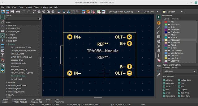
Board Outline and Part Layout
")
The most important step in any layout process is organizing your components and determining the shape of the board outline (not necessarily in that order).
I wanted to keep something with the same basic shape as the Raspberry Pi Pico for this project. However, at the time of writing, the minimum board requirements for DKRed were 1 inch in either dimension. Because the Pico is only about 0.8 inches wide, I had to stretch the sides out to meet the 1-inch minimum.
Instead of wasting space on the breadboard, I decided to add PINs in the silkscreen. Because the PINs are only available on the underside of the Pico, these would at the very least help me create circuits on the breadboard for prototyping.
As you can see, the components are crammed into a Pico-sized shape. This is because I used larger components for hand soldering (except for the RP2040, which only comes in a QFN package). The 0603 decoupling capacitors made routing out of the RP2040 particularly difficult.
The board now has a "tail" with a header for the target SWD connections. I planned to provide two alternatives for connecting the target Pico SWD:
- Solder headers to the Pico's underside on the SWD port and connect them to a header on this debugger shoe. However, this would mean that the Pico would no longer fit on its own on a breadboard.
- To connect the debugger to the target Pico's SWD port, use jumper wires, which means the board had to be slightly extended to accommodate this extra header.
Design Rules
I set the minimum constraints as follows. They were based on the minimum design rules as set out by OSH Park, which is more conservative than what I ultimately plan to build. DKRed offers smaller track width/clearance constraints, but I wanted this board to be able to be produced by nearly any fab house.
The net class parameters are as follows. The default class provided the majority of the traces, but I tried to make the USB power and 3.3V traces as wide as possible (to carry at least 500 mA).
The USB data lines are 0.77 mm wide with 0.15 mm separation on a top layer with a ground plane 1.6 mm below. With the assumptions shown in the screenshot below, this resulted in an ideal differential impedance of 90. See this post for instructions on calculating differential pair trace parameters.
Traces of Routing
The top layer of the PCB is visible here:
Here is the bottom layer of the PCB:
A few words about the design:
- I started by routing USB lines so that they could connect directly to the RP2040 without having to go through another layer (to avoid the 90-degree bends in the vias). While this type of outside-layer USB line routing isn't ideal, it should suffice.
- I then routed the power lines, which are usually wider than the other traces. They also frequently need to make numerous connections, so having a large trunk that branches off to make the necessary connections is advantageous.
- To provide a good current path and aid in heat dissipation, the RP2040 layout guide recommends 9 vias on the middle ground pad to a ground plane. I could only fit 6 vias on the pad due to the crowding of the bottom side traces. I'm hoping this is a good enough compromise.
- The traces to the crystal should be as straight and short as possible while also being length-matched. Because the 0603 capacitors caused crowding once again, I had to route the crystal lines to the side to avoid them. Another compromise that I'm hoping "just works."
- If the user ever wants to disconnect the TX/RX UART debugging lines and VSYS from the target Pico, I provided solder jumpers.
- The fiducials were mostly added out of habit. I doubt I'll ever use a pick-and-place machine to populate this board's components.
- I left out silkscreen markers for pins 0 and 1 to serve as a reminder that the debugger uses those pins.
- I keep REFDES markers for the components in silkscreen because it helps me remember where parts go when I hand-place them.
Gerber Plotting for PCB Fabrication
The Gerber file specifications I used for the plotting step are as follows:
Drill file specifications for KiCad
I kept the PTH and NPTH files separate because I'm hoping that the fabrication process won't plate the mounting holes.
DKRed plates all of the holes. If you intend to use DKRed, you should select "PTH and NPTH in single file."
I compressed these gerbers and uploaded them to Digi-new Key's PCB fabrication process, DKRed. I recommend giving it a try for your next PCB prototyping run. Because there is a minimum order of four PCBs, that is what I ordered.
If you want to see this content in video form, go here:
Conclusion
I hope this helps you begin designing your RP2040 PCB layout!
[source]