KiCad is a free and open-source Electronic Design Automation (EDA) suite originally developed by Jean-Pierre Charras and is now being actively maintained by a group of developers. It has everything needed to create complex multi-layer PCBs as you wish. It has limitless customization options, thanks to the open-source design and scripting tools. KiCad 6 has been released recently. It brings a complete overhaul to the workflow and user interface of all the applications in the suite. That also means KiCad version 6 will be incompatible with version 5 for the most part. KiCad 6 is going to make the platform appealing to an even wider group of people including students and professionals. The V5 had so many ambiguous aspects that many beginners found it a little difficult to start learning it (like I was). But V6 is much more intuitive, straightforward forward, and extensible. KiCad is available for all operating systems and you can download it free from the following link. We also have a dedicated tutorial for installing KiCad version 6 and managing libraries – How to Install KiCad Version 6 and Organize Part Libraries.
How to Install KiCad Version 6 and Organize Part Libraries
In this tutorial, we are going to show you how you can export your PCB designs from KiCad for fabrication. We won’t be giving instructions for creating a schematic or designing a PCB. So we assume you already have a completed design. For this tutorial, we will use our Mitayi Pico RP2040 board design as a reference, with KiCad Version 6 installed on a Windows 11 system.
Gerber Files
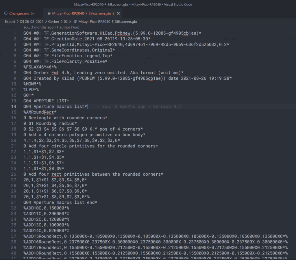
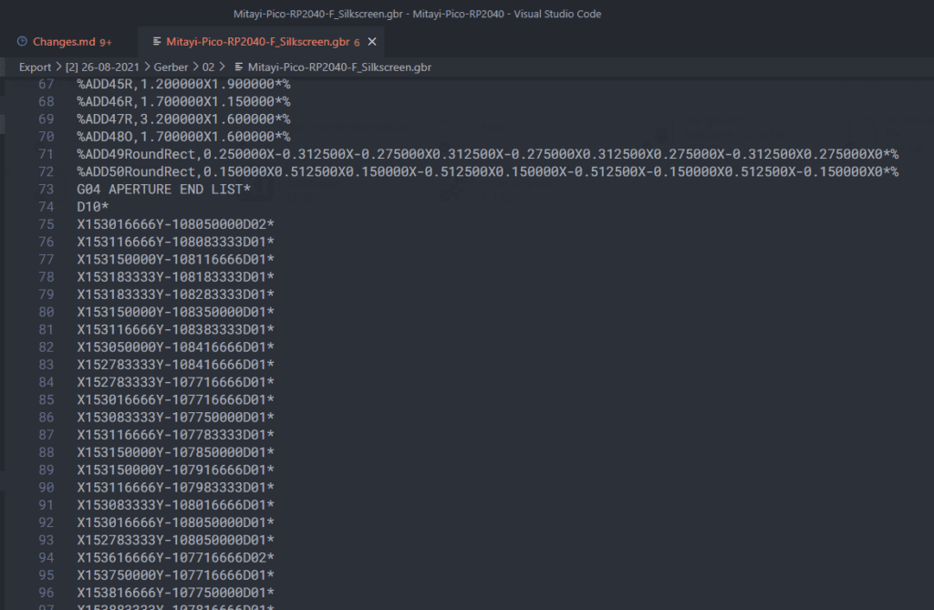
Once you have completed your PCB design, you have to send a few files to the fabrication house to get them printed. These files are different from the original design files you create with KiCad, namely .kicad_sch and .kicad_pcb files. Some manufacturers also accept original design files which they use to generate the files required for fabrication. At the fab house, PCBs are created through a set of consecutive processes. Each process may use a different kind of file for information. All these processes are carried out by computer-controlled machines. So we have to tell the machines what our design looks like and how it has to process it. Gerber is a de-facto standard used by all fab houses to accept PCB fabrication data. Gerber is an open vector standard stored in ASCII format. This means, the contents of the files are in plain text and you can open and view them on any text editor.
Gerber is a vector graphics format. It describes an image as a set of shapes, lines, and points. When you look at each layer of your PCB, that is what you are going to see. Each track is a set of lines of different thicknesses and connecting to pads of different shapes. Therefore Gerber format can describe everything on your PCB. If you open a Gerber file on a text editor, you can see a list of coordinates and other symbols. If you are familiar with G-Codes, you will instantly recognize the similarities. Gerber files are created in a way that is easier for machines to interpret the information. This is unlike, other vector formats such as SVG which only gives preference to appearance and editability.
As we said earlier, each process requires a different type of information. For example, a drilling CNC machine only needs to know where to drill holes with what size. So we just need to send the machine that particular information. To make this easy for the fab house, each layer of our PCB design is saved as a separate file. Each file will be named with that particular layer name and an extension. The layer names and extensions can be arbitrary. Still, KiCad uses a human-friendly format for naming files. It first adds the project name and then concatenates it with the layer name followed by the .gbr extension. For example, a file name could look like this,
LED-Board-F_Silkscreen.gbr
This means it is the Gerber file for the Front side silkscreen for the LED-Board project. You need to have separate such Gerber files for each of the PCB layers if you want the fab house to process it. To make it easy to send and receive files, we usually compress these files as a ZIP archive and send them.
Generating Gerber Files
Before generating the Gerber files, make sure to
- Run the Design Rule Checker (DRC) from Inspect menu and catch and fix all the errors. Some errors can be ignored if you really know what you’re doing (like courtyard overlaps). Everything else has to be fixed.
- Make sure you are using the board design specifications according to the capabilities of the fab house. This includes clearances, track width, hole size, layer count, etc. You can check the manufacturer’s website for a complete list of supported specifications. Mostly, they will specify minimum and maximum values for each parameter. You have to keep this in mind while setting up the board and design rules initially.
- Check all layers individually and make sure you are not missing anything. Things that are violating design rules can be caught easily. But the software can’t tell you about missing items. For example, you might forget to add a version number on one of the silkscreen layers. If you do not do that, it might become hard to keep track of changes to your design.
- Have a common board origin point set somewhere on your design. You can add this using Place drill origin option. This can be later used when exporting Gerber and position (centroid) files. Even though this is not necessary, it is a good practice nonetheless. I usually place an origin point at the bottom left corner of a design. The drill origin point is different from grid origin which is placed on the top left of the sheet by default.
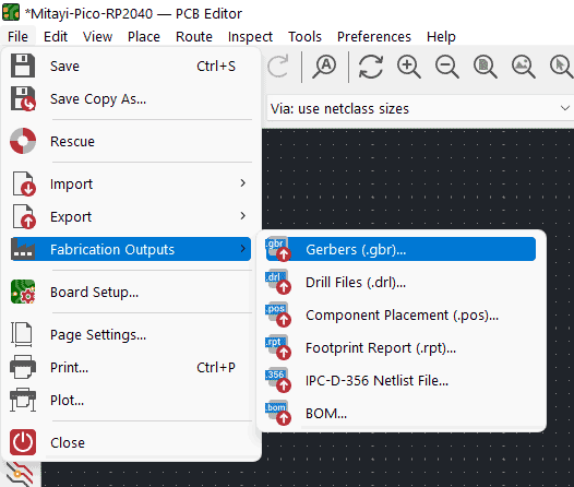
Once you have an error-free design, we can proceed to export the Gerber files. The window to generate Gerber files can be opened from File → Fabrication Outputs → Gerbers (.gbr) or through File → Plot in PCB editor.
This will open the Plot window.
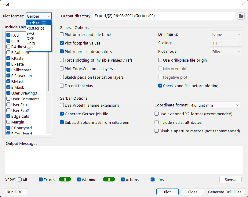
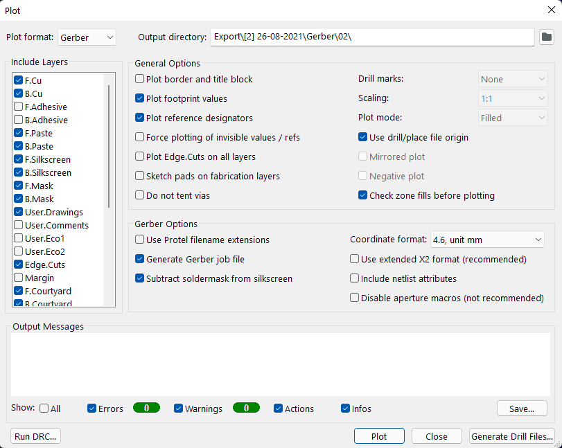
Choose the plotting format as Gerber from the drop-down menu. You also have a few other formats such as SVG, DXF, etc. To set the directory to export to, choose a folder by clicking the icon on the top right. We usually store all Gerbers on a folder called Export inside which we will create a folder for that day and a folder named Gerber inside it. You might create multiple sets of Gerber files a day. In that case and if you want to keep those old files, you can create additional folders inside them. Otherwise old Gerber files will be replaced with new ones. Below is how we create the folders.
Export → [1] 27-05-2021 → Gerber → 01
File names and numbers are the easiest ways to keep track of your exported files. Believe us, it is going to be really important. You don’t want to send the wrong Gerbers to the fab house only to realize the mistake you have done after printing 1000s of PCBs. If you look at the way the folders are created, the folder names can be concatenated with the project name and version and made to a single name for that particular set of Gerber files.
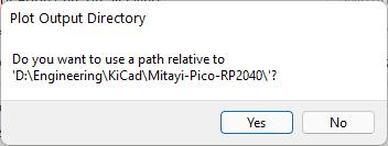
When you choose the folder, KiCad will ask if you want to use a relative path. Click Yes for that. Next is to choose the layers you want to export. For single-layer designs, you only need either a Front or Back set of files. For double-layer designs, you need both sets. You will see more layers if you have a multi-layer board. So choose the layers accordingly. Any additional layers that you choose, that are not used by the fab house will be ignored. For a typical two-layer design, you need,
- F.Cu – Front copper layer
- B.Cu – Back copper layer
- F.Mask – Front mask layer
- B.Mask – Back mask layer
- F.Silkscreen – Front silkscreen with all the labels
- B.Silkscreen – Back silkscreen with all the labels
- Edge.Cuts – the board outline and cuts
Optional layers can be,
- F.Paste – tells where to apply solder paste on front side
- B.Paste – solder paste layer for back side
- User.Drawings – you can add dimensions and other reference drawings here
- User.Comments – any additional information you want to share
- F.Courtyard – 2-dimensional bounding boxes for each component
- B.Courtyard – same for back side
Now we have a set of options grouped into two sections; General Options and Gerber Options. For both, choose the settings as shown below.
You can hover over each option and it will give you some additional information on what that setting means. But let us also explain them.
General Options
- Plot border and title block – every design will be contained inside a page layout. This can be standard A4, A3, etc., or any custom templates. If you want to plot the page layout on all Gerber files, you can enable this checkbox. Most times, you don’t need this. So uncheck it.
- Plot footprint values – footprints can have multiple parameters associated with them such as the component reference, value, etc. If you want the component value to show up on the silkscreen or other layers, you can check this box.
- Plot reference designators – you need to enable this checkbox if you need the reference designators (R1, R2, C1, C2, etc.) to appear on the Gerber files.
- Force plotting invisible values/refs – KiCad allows you to hide items on the editors. By default, these are also not included in the exported files. But if you want these items to appear on the Gerbers, you can enable this checkbox.
- Plot Edge.Cuts on all layers – the board outline is only present on the Edge.Cuts layer by default. But if you want them to appear on all layers, you can enable this checkbox. This is usually not necessary.
- Sketch pads on fabrication layers – if you’re exporting the fabrication layers (F.Fab etc) you can also include the pads on them. By default, they are not included. This is also not necessary.
- Do not tent vias – tenting is the process of covering vias with solder mask material. If you do not want to cover the vias but expose them, for example for testing, you can enable this checkbox.
- Drill marks – drill locations will not be marked.
- Scaling – it is kept at its actual size (1:1).
- Plot mode – shapes will be filled.
- Use drill/place file origin – I mentioned the drill origin before. If you have manually set a drill origin already, you can ask KiCad to use it for the Gerber files also. Even if you did not set a drill origin and unchecked this option, everything will be fine because there will be still a grid origin.
- Check zone fills before plotting – KiCad does not automatically refill zones after you make a change to the design. It has to be done manually. So it is a good practice to keep this box checked for automatic filling of the zones.
Gerber Options
- Use protel name extensions – some systems use different file extensions for Gerber files. For example .GBL for bottom (or back) layer. These are no longer common and you can keep the .gbr extension for all the files by unchecking this option.
- Generate Gerber job file – once the Gerbers are created, an extra file is created with the extension .gbrjob that describes the project, board layout, layer stackup, etc. This might help some programs and fab houses to better understand and verify the Gerber files you send.
- Subtract soldermask from silkscreen – KiCad can subtract two graphic layers and include only the result inside the files. Subtracting soldermask from silkscreen will help to remove any silkscreen items from places on the board without soldermask, including pads. This can improve solder paste application and solderability. So keep this checked.
- Coordinate format – set this to 4.6, mm format so that each coordinate will have 4 places on the left side of the decimal point and 6 places on the right side of the decimal point. Units will be in millimeters, part of the most sensible unit system.
- Use extended X2 format – the Gerber has an extended specification called the X2 format or RS-274X compared to the standard Gerber called RS-274D. Most manufacturers accept both formats. Check with your fab house which format they want and choose this option accordingly.
- Include netlist attributes – netlist is a list of all the interconnections on your PCB design. It describes which component is connected to where. This information can help some systems to detect errors in your design and even be used for automated inspection of your PCBs. You usually don’t need this.
- Disable aperture macros – aperture macros are an easy way to include items that repeat at so many places inside the Gerber files. Using aperture macros will reduce file sizes. So you usually want to keep this unchecked.
Once the options are set, we can move on to clicking some buttons. You can run DRC for a final time with Run DRC button. Plot is for plotting the Gerber files to the selected directory. Any messages or info during the operation will be printed on the Output Messages window. You can save the log with Save button.
Since we have created the Gerber files, you might think that was the end of it. But we are not done yet. We said the Gerber files are graphics files. They describe shapes. But they don’t describe a very important thing; drilling. CNC drilling machines need to know where to drill each hole and the drill sizes to use. This information is not part of the Gerbers and should be generated separately. The button Generate Drill Files is for that. Clicking the button will open a new window.
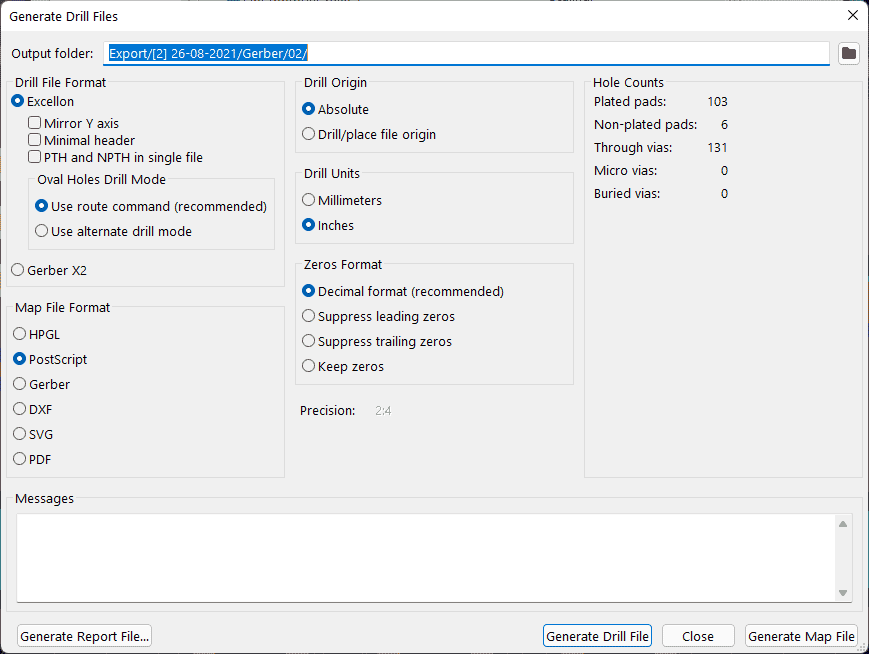
You can keep the drill files together with Gerber files. So you don’t need to change the directory. For now, all options can be kept as above, unless your fab house recommends something else. Any mistakes you do here can spoil your PCBs. But don’t worry too much thinking if you would make a mistake or not. We will review the Gerbers once we have exported them. So keep calm.
Clicking Generate Drill File will add a few more files to the directory. Clicking Generate Map File will create a visual representation file of the drill points. This file can be opened with any standard vector editing software. This file is optional and can help in creating assembly drawings, which we will talk about later.
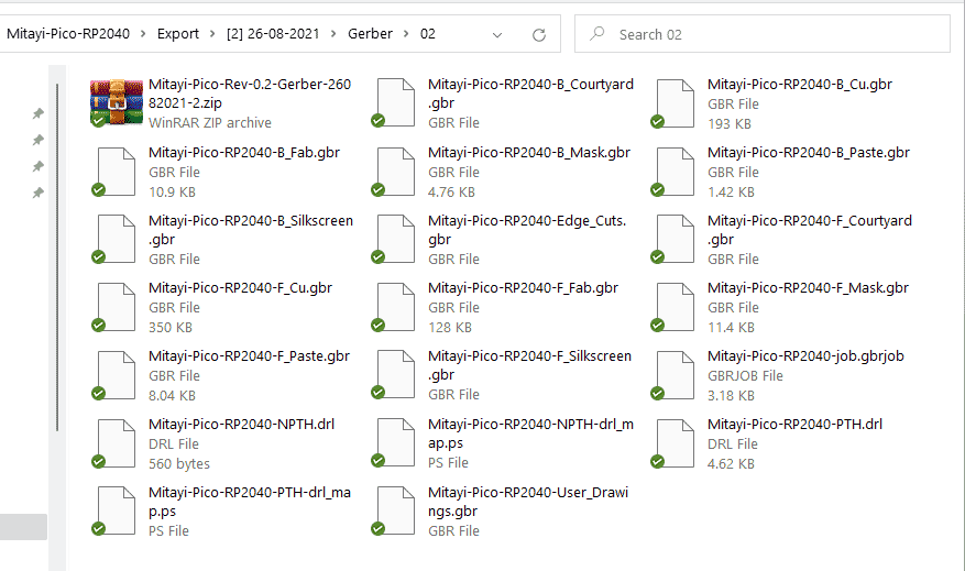
See the set of Gerber files we have exported for our Mitayi project.
Also, observe the ZIP file. It contains all the files required for fabricating the PCB. We have named it with the project name, revision, export date, and sequence number. You can follow that or something similar.
Verifying Gerber Files
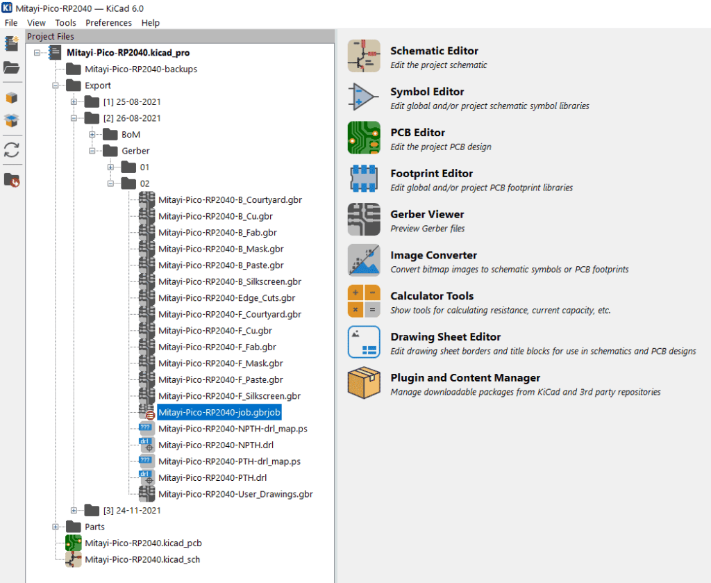
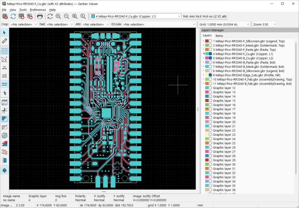
Now that you have exported the fabrication files, you can proceed to send them to the fab house if you feel too confident. If you have the slightest doubt about the files, you can view them with any Gerber viewers and verify them. Luckily, the KiCad EDA suite has a Gerber Viewer. It is a standalone application like the rest of the applications. You can open the Gerber Viewer from the main dashboard or click on any Gerber files. If you have generated a Gerber job file, clicking on it will open all the Gerber files together.
The File menu has a few options to open different types of files. You can open the Gerber files directly, or open a ZIP file. You can also open the drill files (Excellon files) separately to also see the holes. Check each layer individually and verify they are as you expect. You have a few tools on the left to change to different view styles. Take your time and verify, that’s what we are saying.
Sending to Fab House
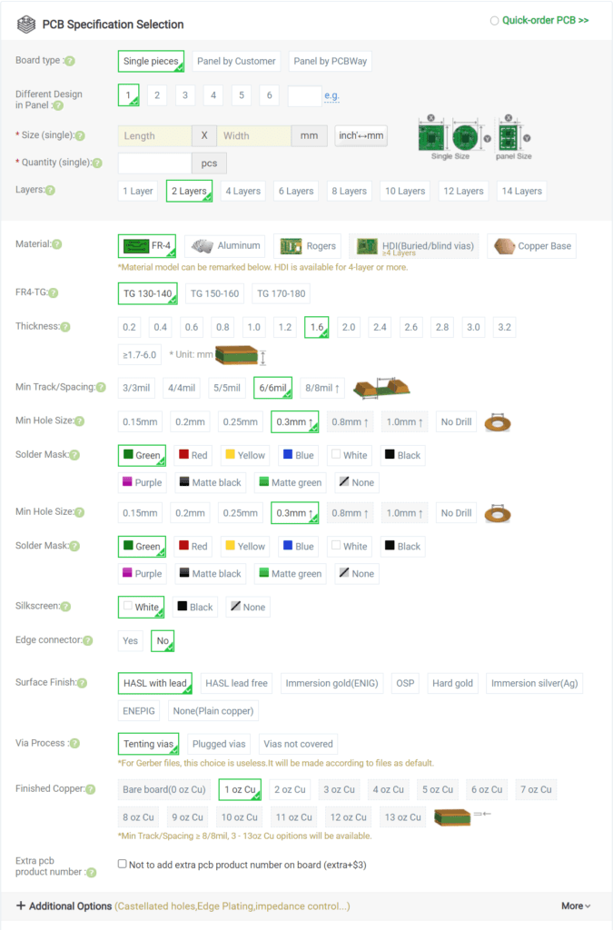
Different manufacturers have different methods for accepting fabrication files. Some have a web interface where you can upload the Gerber files as a ZIP and it will show a preview of the board. The interface will automatically detect many parameters such as dimensions, number of signal layers, etc. Some don’t have such interfaces and uploaded files are verified manually.
In all cases, a ZIP file is the best format for sending Gerber files. After uploading the files, you will need to manually enter some of the parameters for fabrication, such as the soldermask color, since that kind of information is not present in the Gerbers. Once an order is approved, sit back and relax while your PCBs are fabricated.
Check The PCBs
Once you receive the PCBs, check them for quality issues.
- Check how your PCBs are packed. Usually, PCBs are packed inside a vacuum-sealed plastic covering. The fab house may insert paper sheets in between the PCBs to prevent them from getting scratched.
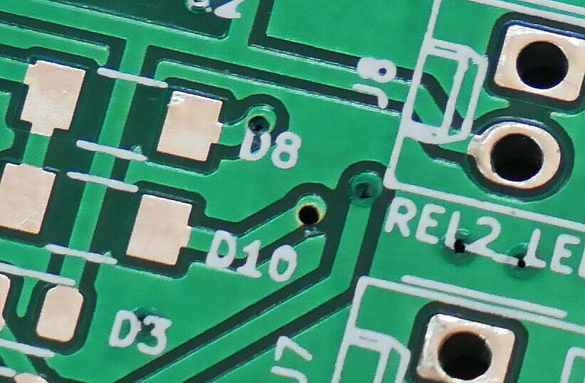
- Check if the hot air solder leveling is done properly if you chose the HASL process. If this is not done properly, solder residue can remain trapped inside plated through-holes and make it difficult when inserting components. For SMD pads, if the hot air leveling is not done correctly, the surface can be uneven and cause soldering issues.
- Check if the drilling is done properly. The drilling process may not be always precise for some or all PCBs. In such cases, holes can be shifted from their actual drill positions. If there is too much shifting, the PCBs may become unusable, and may still pass the electrical test. If you find the drilling quality of a manufacturer is not good enough, it is better to not use their services anymore.
- Check if there is any significant solder mask layer shifting. This can cause SMD pads to be unusable. Also, check the solder mask consistency. If the layers are not consistent in color and thickness, that may be indicating poor processes and machines used.
- Check the quality of the silkscreen. Manufacturers use different methods for printing silkscreen and depending on the method, the quality can be different. Some manufacturers such as OSH Park deliver precise silkscreen text even for smaller font sizes.
- Ask for a PCB quality test report. This data may include flying probe test results.
That’s all we have to share for now. If you have any questions or if you think we missed something, post them in the comments. In the next post, we will show you how you can export your PCB design for automated assembly.


