KiCAD Projects: MITAYI Pico RP2040 r0.2 an open-source microcontroller development board

CIRCUITSTATE Electronics LLP offers the MITAYI line of RP2040-based microcontroller development boards. The first book in this series is MITAYI Pico. We were pleased with the functionality and price of Raspberry Pi's first microcontroller offering. With the early availability of their products, Raspberry Pi also performed a fantastic job of offering documentation and development help. These factors led to the RP2040 microcontroller and Pico development board dominating the maker market.
Our desire to incorporate the new microcontroller into our designs led to the creation of Mitayi. The first draft of the design is the MITAYI Pico r0.2. The open-source EDA tool KiCad will be used to design every board in the Mitayi series. This tutorial will take you step-by-step through the manual assembly, testing, and schematic design processes for the Mitayi Pico board.
Mitayi Pico RP2040 v0.2 Features:
- RP2040 dual-core, 133MHz ARM Cortex M0+ microcontroller.
- 16MB Flash memory in a SOIC-8 package.
- Dual USB connector options; Type-C and Micro-USB.
- Dual voltage regulators; AMS1117 and MIC5219.
- Reset button.
- Solder jumper for debugging LED.
- Breaks out all GPIO pins (not pin-compatible with RPi Pico).
- Uses 0402 or larger SMD packages.
- Component references on the silkscreen.
- Same dimensions of 21 mm x 50 mm, with almost the same positions for mounting holes.
- Completely open-source design made with KiCad 6.
Our first line of microcontroller development boards is called MITAYI. The word "candy" in Malayalam, (IPA-EN: mihyi), is where the name originates. For our boards, we wanted a Malayali + Indian flavor. Hope it turns out okay. Only the Raspberry Pi RP2040 microcontroller will be used in Mitayi boards. This series will begin with Mitayi Pico. It will be followed by the Mitayi Nano, Mitayi Micro, Mitayi Stamp, and more products.
The Mitayi Pico has some visible enhancements but is still made to seem quite similar to the official Pico. The initial design version for which we attempted to obtain PCBs was revision 0.2. PCBWay generously provided the top-notch ENIG PCBs for r0.2. PCBWay is a PCB manufacturer from China with a full production pipeline for PCB Fabrication (all standards), Component Sourcing (turnkey, consigned, and kitted), and PCB Assembly. As the majority of our readers already know, or if you are new to PCB designing (single, double, flex, etc).
Additionally, PCBWay provides 3D printing services utilizing both metals and plastics. The open-source EDA software KiCad is sponsored at the Silver Level by PCBWay. Even more giveaways and design/project competitions are periodically held by PCBWay for creators all over the world as if that weren't enough. To receive information on the competitions and to enter to win free PCBs and other cool stuff, follow PCBWay on their social media channels. We appreciate PCBWay's sponsorship of Mitayi Pico's PCBs.
The Mitayi Pico design in Revision 0.2 is not flawless, as one might anticipate. We unavoidably had to make mistakes and implement additional design enhancements. As a result, r0.2 is not prepared for production. R0.2 must only be used as a reference. With the impending production-ready design r1.0, we anticipate resolving all difficulties, and we'll start selling the boards.
This article is only intended to provide documentation of the Mitayi Pico r0.2 design process. We'll be updating the board design regularly and releasing those updates to our GitHub. As a result, bookmark and star the project on GitHub. It will also be possible to get the source files for this open-source project at CADLAB.io, which is a program you should certainly check out.
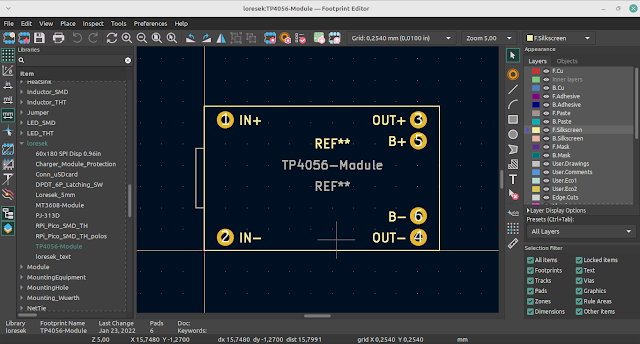
Schematic Design

The Mitayi Pico schematic was created using KiCad version 6, and it closely resembles the official Pico schematic diagram and design standards. Additionally, we looked into Shawn Hymel's Pico Debugger Shoe design. Let's look at each block in the Mitayi Pico r0.2 schematic.

The working voltages for the RP2040 microcontroller are 1.1V for the core and 3.3V for everything else. We do not need to supply both voltages. An inbuilt 1.1V low drop regulator is present in the RP2040 (LDO). The VREG-IN pin and all IOVDD pins require a +3.3V supply. The output of the VREG-VOUT must be linked to each of the DVDD pins, while the VREG-IN serves as an input to the 1.1V LDO. We also need to connect the USB-VDD pin to the 3.3V supply. The supply for the internal ADC is accepted on the ADC-AVDD pin.
The ADC is extremely sensitive to interference, drift, and supply noise. Therefore, you can utilize a separate low noise, high precision voltage reference designed specifically for the ADC if you want the highest level of accuracy in your ADC readings. The ADC-AVDD pin on the official Pico schematic has a capacitor and current-limiting resistors. The pin is provided with a solder jumper in the Mitayi Pico r0.2 schematic so that you can either provide your supply or connect the ADC-AVDD pin to the 3.3V supply.
We started from scratch when designing the RP2040 schematic symbol and grouped pins with related functionalities. A 27R resistor is connected in series with the USB data channels.
Flash Memory

The W25Q128JVSSIQ from Winbond in SOIC-8 packaging is the flash memory that is being used. To start the board in boot mode, the QSPI SS (Chip Select) pin is attached to the USB Boot solder pad. When the RP2040 powers up, the microcontroller immediately pauses loading and carrying out any instructions from the flash chip if the QSPI SS pin is low. Instead, it will list itself as a mass storage device that is open to receiving new firmware (with the aid of a Read-Only firmware). The RP2040 will simply replace the flash memory with the new file and exit from program mode when we drag and drop a UF2 file to the disk.
The optional pull-up R1 should be 10K if used. The QSPI SS pin is wired to a push button in the standard Pico design. Instead of using a push button, we chose to use a solder pad and reserve it for the RESET function. However, that was a poor design decision. In the upcoming design, we'll have buttons for BOOTSEL and RESET. When you mess up your firmware, the BOOTSEL and RESET buttons might help you "save" your RP2040.
USB Type-C Receptacle

The Mitayi Pico r0.2 design offers Type-C USB (MPN: Korean Hroparts TYPE-C-31-M-12) and Micro USB (MPN: Molex 105017-0001) port options. With two data pins (USB D- and USB D+) and two supply pins, the Type-C receptacle serves as a USB 2.0 interface. The RP2040's USB pins are coupled with identical bus pins for testing. The two 5.1K resistors on the CC1 and CC2 lines enable the detection and proper current sourcing of the USB device.
Since they are not required, the auxiliary bus pins SBU1 and SBU2 are not connected. The Schottky diode MBR1020VL connects the 3.3V voltage regulator to the VBUS, which delivers a 5V supply from the USB. The diode guards against reverse supply input for the USB host.
USB Micro Receptacle

The signals used by micro USB and Type-C outlets are identical. However, since you can only solder one of them at a time, this won't be a problem. If you can't obtain Type-C connectors or wish to keep the board's price low, the USB mini is offered as a backup connector. But happily, since 16-pin Type-C connectors can be found in India for as little as INR 5, you won't ever need to utilize micro USB connectors again.
Main Voltage Regulator

The main 3.3V regulator is a Microchip MIC5219-3.3YM5. The LDO has a 500mA maximum output current. Due to the low drop, you can directly power the board with a 3.7V Li-Ion or LiPo battery. If you want to use a similar regulator with a different pinout, you can configure the regulator by using the solder jumpers VR1 IN, VR1 CE, and VR1 BP.
We included these since LCSC sells a lot of identical, inexpensive voltage regulators made by Chinese manufacturers. However, we believe the upcoming design won't require them. You can turn the board on or off by using the V EN signal to enable or disable the voltage regulator.
Secondary Voltage Regulator

You can use this as a backup 3.3V regulator in place of the more expensive MIC5219. The voltage regulator output can be connected to the 3.3V rail via the VR2 OUT. Additionally, this won't be incorporated into the Mitayi Pico design's subsequent iteration.
Reset

Both a push-button and a pin are provided for the RP2040's reset function. There is no specific reset pin on the official Pico. We utilized a 2-pin SMD type - 3x4x2mm SMD Tactile Switch - often seen on ESP32 boards for the push-button.
Crystal

We are utilizing a 12MHz SMD type crystal in this instance. However, the incorrect part number is ABLS-12.000MHZ-B4-T. It was initially a bigger SMD crystal, but we switched it out with one from YIC called 12M20P2/XT324-10/10. Here, too, we made a grave error. A 4-pin SMD crystal, the 12M20P2/XT324-10/10 has ground connections on pins 2 and 4 and signals on pins 1 and 3. So, for Y1, we employed a 4-pin footprint. Furthermore, the schematic clearly shows that Y1 only has two pins. We had to manually cut tracks and rewire to resolve this problem.
Fortunately, the capacitor numbers we utilized are accurate. The load capacitance of the 12M20P2/XT324-10/10 is 20pF, and to obtain that value, we used ceramic capacitors with a value of about 30pF. Since 27pF was readily available, we chose it. The needed capacitor value is calculated as follows:
- C18, C19 = 2 * (CL - Cs)
- CL = 20pF, Cs can be ~5pF
- C18, C19 = 2 * (20 - 5) = 30pF
Debug LED

A solder jumper called DEB EN connects the debug LED to GPIO25, allowing you to detach it if you require the pin for something else in the future.
Pin Headers

The official Pico and Mitayi Pico have different pinouts. This is because not all of the GPIO pins are broken out by the official Pico because some of them have other uses. We intended to limit the GPIOs' additional usage while still enabling the user to utilize all of the available pins. The Mitayi Pico offers some compatibility with the official Pico and deconstructs all the GPIO pins. For instance, the pin assignments for VBUS, VSYS, GND (pin 38), V EN, and 3V3 OUT are all the same. It appears that we can also create an identical AREF pin. On the Mitayi Pico, the SWD pins are also located in the same location.
PCB Design

KiCad 6 was used to create the PCB. To make them easier to manufacture, we chose a 2-layer design. The official Pico was set up in the same position and orientation as RP2040. The minimum clearance and default track thickness were both 0.2 mm. The diameter and drill size of every via are the same for 0.5mm and 0.3mm. Simply a 20-pin pin header footprint with a 2.54 mm pitch was altered for the pin headers with castellated holes. A castellated hole will be made if the edge of the PCB passes through the center of a plated hole. It requires minor cleaning after the accurate drilling or scoring.
The Type-C and Micro USB connector stacking was simpler than we anticipated. When stacked on top of one another, the footprints we used did not interfere with one another. Routing was also simple because similar signal types were facing one another directly.

On the official Pico, the USB data lines are impedance matched. This is so because there is a sizable gap between the RP2040's USB pins and the USB connector. The need for length matching, impedance matching, differential routing, and other techniques increases when you need to route high-speed signals. The built-in calculator tool in KiCad can be used to figure out the dimensions and other specifications of various transmission line types.
Coupled Microstrip Lines or Differential Microstrips are the two types of transmission lines used for USB, depending on whether the signals are odd or even (when signals are differential). Two traces with identical trace lengths and identical spacing will be present in this. A consistent ground plane (Ground pour/fill) should be placed underneath the traces as well. Any Microstrip calculator can be used to figure out the width and spacing of these traces.
Instead of the usual 50 Ohms, a differential USB line requires impedance matching of 90 Ohms. We can enter a few values into the calculator, and it will display the trace widths and spacing necessary to obtain the 90 Ohms impedance. For a 2-layer FR4 PCB with a thickness of 1 mm, we utilized 0.8 mm trace width and 0.17 mm spacing. This results in an acceptable differential impedance of about 89 Ohms.

Without minor adjustments, connecting thick tracks to small pads is impossible. One approach is to taper the track width until the connection is made and it matches the pad. Another approach is to join the bigger track with a smaller-width track. The latter was applied. As long as the length of the feature is less than the critical length, doing so wouldn't significantly affect the impedance matching.

PCBWay provided the PCBs for Mitayi Pico r0.2. For the manufacture, we followed the aforementioned criteria.

Download
We will save the entire set of design files to a root folder called Export in addition to the Git version control. There will be other folders for each version or day inside of that one. This will make it simple to locate and launch individual design files at the same time as needed. Download all r0.2 design files via the link below:
KiCAD Projects: MITAYI Pico RP2040 r0.2